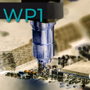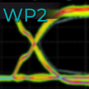
WP2 – Signal integrity (SI) and power integrity (PI) of FPGA chips and PCBs
The aim of this work package is to evaluate the impact of SI and PI on FPGA chips, including the quantification of effects caused by EMI on high-speed digital circuits during operation. This will include: i) the design rules for the location of components (e.g. integrated circuits) on chip and on PCBs based on in-situ assessments of performance; and ii) the development of methods to validate test data and assess parasitic effects due to components operating simultaneously in close proximity on chip.
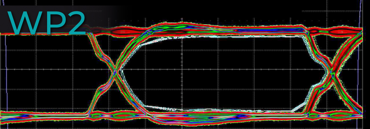
WP2 will develop traceable characterisation methods for parameters in order to evaluate the SI and PI on FPGA chips and on dedicated PCBs. These methods will also include the quantification of effects caused by EMI on high-speed digital circuits during operation. Measurement procedures will also be devised to carry out in-situ assessments of performance, which will support the development of methods to assess parasitic effects due to components operating simultaneously in close proximity on chip. Finally, FPGA programming will be used to evaluate in situ and in operando impact of location of functions on chip and on PCB.
The work package is divided into three tasks, the aims of which are:
- Task 2.1. to develop metrology for SI and PI applicable to chip level of FPGA circuits.
- Task 2.2. to develop metrology for SI and PI applicable to FPGA boards up to 50 GHz.
- Task 2.3. to develop traceable measurement procedures to evaluate EMI on high-speed digital circuits during operation and to assess parasitic effects due to components operating simultaneously in close proximity and on chip.
WP Leader
Djamel Allal, LNE
email: djamel.allal@lne.fr